Category

All

  • femtosecond laser
    femtosecond laser
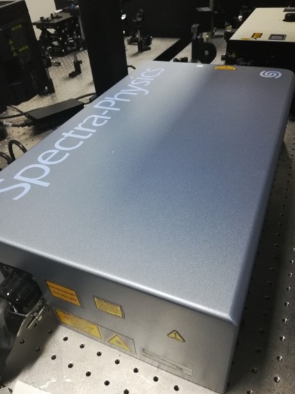
    A femtosecond laser is a pulse laser. Femtosecond is the duration of the pulse. This is not the same as the frequency of the pulse. The frequency of the pulse is the number of pulses that the laser sends out in 1s. The femtosecond laser's resolution of time is much higher than that of film and television equipment. It has been calculated that this femtosecond laser has obtained the shortest pulse in the world that human beings can obtain in the laboratory. Through it, we can see faster and more subtle movements, such as the process of photosynthesis in green plants, the process of dividing cells, the process of electrons moving around atoms, and so on.

  • Fourier Transform Infrared Spectrometer
    Fourier Transform Infrared Spectrometer
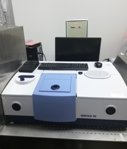
    Fourier transform infrared spectrometer is mainly composed of Michelson interferometer and computer. The main function of Michelson interferometer is to divide the light emitted by the light source into two beams to form a certain optical path difference, and then combine them to produce interference. The obtained interferogram function contains all the frequency and intensity information of the light source. The frequency distribution of the intensity of the original light source can be calculated by Fourier transform of the interferogram function with a computer. It overcomes the disadvantages of the dispersion-type spectrometer, such as low resolution, small output of light energy, narrow spectral range and long measurement time. It can not only measure the absorption and reflection spectra of all kinds of gas, solid and liquid samples, but also can be used for short time chemical reaction measurement. At present, infrared spectrometer has been widely used in electronics, chemical industry, medicine and other fields.
  • inverted microscope
    inverted microscope
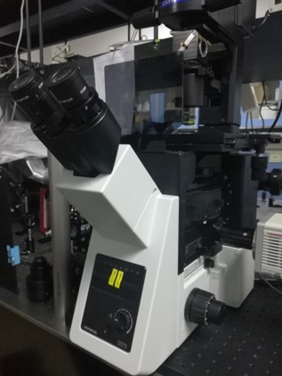
    Inverted microscopes perform the same function as magnifying glasses: they make a larger image of a small object close at hand for the human eye to see. It's just that a microscope can have a higher magnification than a magnifying glass. The object is in front of the objective lens and is farther away from the objective lens than the focal length of the objective lens, but less than twice the focal length of the objective lens. Therefore, when it passes through the objective lens, it must form an inverted magnified real image A'B'. A transpose B transpose near F2. Then it is enlarged into A virtual image A "B" by the eyepiece for the eye to observe. An eyepiece functions as a magnifying glass. The only difference is that what the eye sees through the eyepiece is not the object itself, but a magnified image of the object made by the objective lens.

  • Princeton  Spectroscope
    Princeton Spectroscope
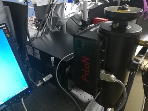
    PyLoN supports a range of cryogenically cooled CCDs with flexible readout design and 120-1100 nm sensitivity.It offers high-performance spectroscopy with fast spectral rate and lowest system read noise

  • PECVD ( Plasma Enhanced Chemical Vapor Deposition )
    PECVD ( Plasma Enhanced Chemical Vapor Deposition )
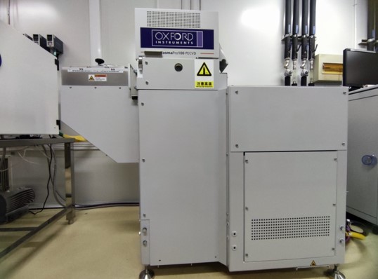
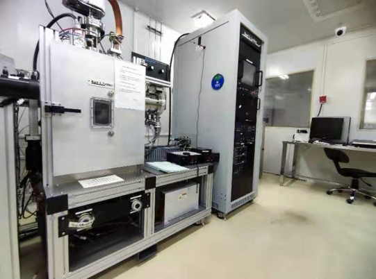
    PECVD: By means of microwave or radio frequency ionization of the gas containing the atoms of the film component, the plasma is formed locally, and the plasma has strong chemical activity, which is easy to react, and the desired film is deposited on the substrate. In order to allow the chemical reaction to take place at lower temperatures, the activity of the plasma is utilized to facilitate the reaction.

  • Ion beam assisted deposition and coating equipment
    Ion beam assisted deposition and coating equipment
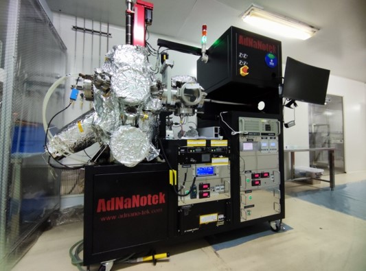
    By using accelerated electron bombardment, the kinetic energy of the electron is converted into heat energy to make the coating material evaporate and form the film. It can vaporize refractory metals or compounds to produce high purity films.

  • Magnetron Sputtering PVD
    Magnetron Sputtering PVD
    By the interaction of magnetic field and electric field, electrons move in a spiral shape near the target surface, thus increasing the probability of producing ions when electrons collide with argon gas. The generated ions collide with the target surface under the action of electric field and sputter out the target material, which is used to prepare metal, semiconductor, insulator and other materials.

  • Focused Ion beam microscope
    Focused Ion beam microscope
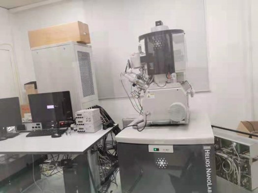
    An electric lens is used to focus the ion beam into a very small size to bombard the surface of the material to achieve stripping, deposition, injection, cutting and modification of the material. With the development of nanometer technology, nanometer manufacturing industry develops rapidly, and nanomachining is the core part of nanomachining, and the representative method of nanomachining is focused ion beam. In recent years, focused ion beam (FIB) technology has become the main method of nanoscale analysis and manufacturing by using high intensity focused ion beam to perform nanomachining of materials, which is observed in real time with high power electron microscope such as scanning electron microscope (SEM).

  • Contact lithography machine
    Contact lithography machine
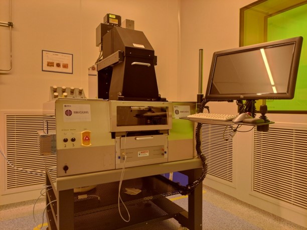
    Contact lithography machine is a kind of process test instrument used in the field of information science and system science, energy science and technology, electronics and communication technology. It is often used in micro-nano processing.

  • Optical coating system
    Optical coating system
    Optical coating machine is a kind of technology test instrument used in the field of information science and system science, physics, to achieve the precise preparation of multilayer optical film.

  • Electron Beam Evaporation
    Electron Beam Evaporation